
I’ve given up on trying to post periodically here. Let’s see if this brave act of reverse psychology has some effect on my productivity.
Introduction
Recently, I’ve started working on firmware for a three-phase frequency inverter. While this is absolutely no technological revolution on the grand scheme of things, it’s certainly new ground for me – and deserves some proper notetaking. So, before we dive into anything, let’s do a quick overview. What’s a frequency inverter? Very broadly, a frequency inverter, or Variable Frequency Drive (VFD), is a device that takes a periodic input signal with a certain frequency and generates a periodic output signal with a different, controllable frequency.
Practically, we’ll be almost always dealing with sinusoidal (or sinusoidal-ish) input and output signals. The reason for that being that mains power is sinusoidal, and most loads we’re interested in (i.e., induction motors) require some form of rotating magnetic field that can be canonically generated by a superposition of sine waves. Also, on a typical industrial context, mains power is three-phase AC (figure below, left). On this setup, you have three sinusoidal waves, 120º apart. There are a lot of inherent advantages to this arrangement, including a reduction in wire count and gauge, easier hookup to loads and so on. Three-phase AC is a whole world in and of itself, and since I’m not qualified to give you a tour of it, I’ll leave its further comprehension as an exercise to the reader (ElectroBOOM to the rescue).
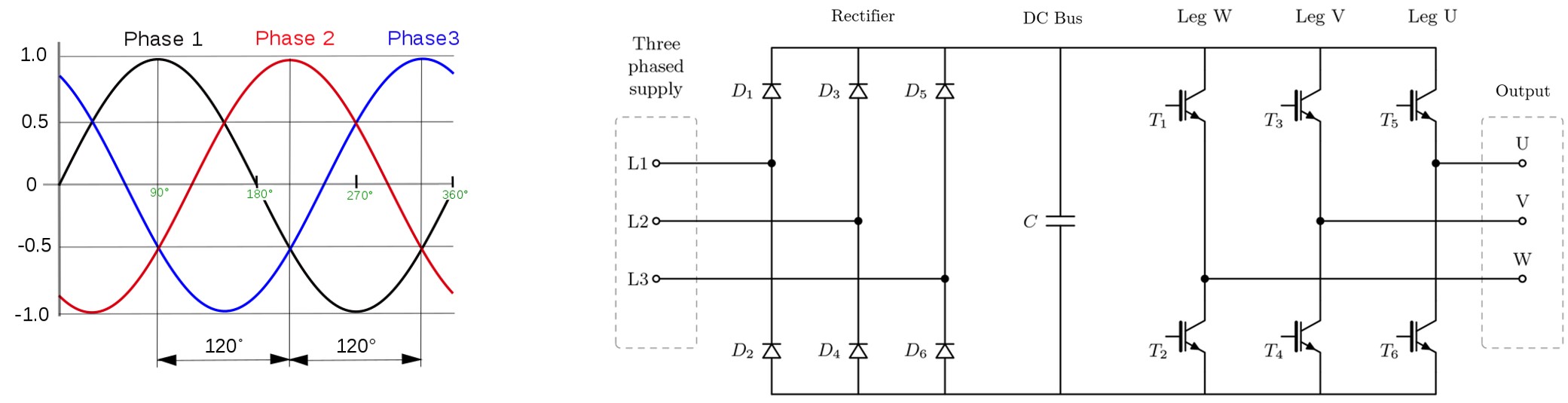
On the above figure, to the right, we see a simplified representation of a three-phase VFD: first, the input three-phase AC signal is rectified into a constant(-ish) DC potential; then, using some form of switching element (e.g., MOSFETs, IGBTs) an output three-phase signal with the desired frequency is generated by combining the output of the U, V and W legs of the circuit. This, in itself, is already the first challenge to be faced: $T1, T2, … T6$ are most efficient when operating in the saturation region – i.e., as hard switches, either fully on, or fully off. So, how can we produce a sinusoidal output signal via elements with a binary behavior?
Mathemagics: the sideways ZOH
First and foremost, by looking at the above diagram, it is very clear that no two switches on the same leg should be simultaneously active at any time – that would configure a short circuit, raise some magic smoke and probably pop a breaker. With that out of the way, we assume that each leg of the VFD can only be in one of two states: on (i.e., upper switch closed, bottom one open), or off (upper switched open, bottom one closed). This means each phase’s output can be either tied to the DC bus’ voltage, or to the ground/reference potencial.
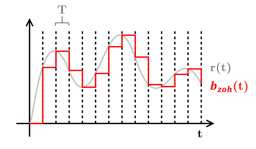
So, we are interested in (re)constructing a signal using nothing but switches. Some quick googlin’ points us to a very commonly used technique for signal reconstruction, called Zero-Order Hold (ZOH). This technique allows us to create a continuous-time signal from a discrete-time signal (e.g., a series of numeric values), by holding constant each of its values for an interval $T$, as shown in the figure below. In a certain sense, this is akin to a Riemann sum, with the area under each sample acting as an approximation to the area under the original signal at that interval. By setting an appropriate $T$ according to the Nyquist-Shannon sampling theorem, the output $b_{zoh}(t)$ signal will contain the harmonic content of the original $r(t)$. Of course, higher harmonics will be present due to the hard transitions between levels, but these should be filtered off.
In this definition, the signal $b_{zoh}(t)$ has arbitrary, non-discrete values (i.e., the sampled values of $r(kT), k \geq 0$). However, as mentioned before, the VFD we’re dealing with only allows each phase to be in two discrete states: fully on or fully off. How to circumvent this? While we can’t control the VFD’s amplitude, we can control how long we keep the signal on or off – that is, each pulse can have its width modulated (PWM). Thinking along the lines of the aforementioned Riemann sum, we can try “tipping” each sample of $b_{zoh}(t)$ on its side. So, assume that on an instant $t_0$, our signal of interest $r(t_0) = f_0$ (figure below, left). Our reconstructed signal $b_{zoh}(t)$ will hold the value $f_0$ during the interval $T = t_1 – t_0$, which results on an area $A_0 = (t_1 – t_0)f_0 = Tf_0$.
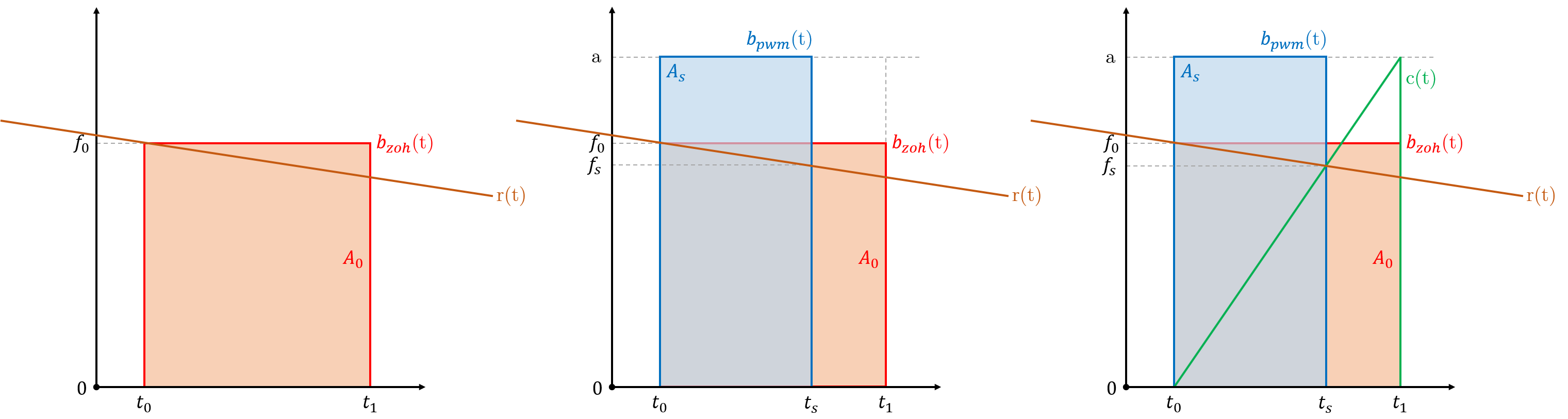
Since our VFD signal $b_{pwm}(t)$ can only be 0 or the maximum amplitude $a$ (figure above, center), we wish to find the instant $t_s$ where the area $A_s = (t_s – t_0)a$ approximately matches $A_0$. This can be written straightforwardly as
\begin{align*} A_s &= A_0 \\ a(t_s – t_0) &= f_0(t_1 – t_0) \\ t_s &=\frac{f_0}{a}(t_1 – t_0) + t_0 \end{align*}
By plugging the above expression for $t_s$ into $A_s = (t_s – t_0)a$, we get $A_s = Tf_s$. For an adequate interval $T$, we can safely assume that $f_0 \approx f_s$, and thus, $A_s \approx A_0$. Hooray. Now, by also assuming that $0 < r(t) < a, \forall t$, we can write the unsurprising relationship between $t_s$ and $f_s$, in each interval $T$, as
\begin{align*} f_s = a\frac{(t_s – t_0)}{(t_1 – t_0)} && \forall t, t_0 \leq t < t_1 \end{align*}
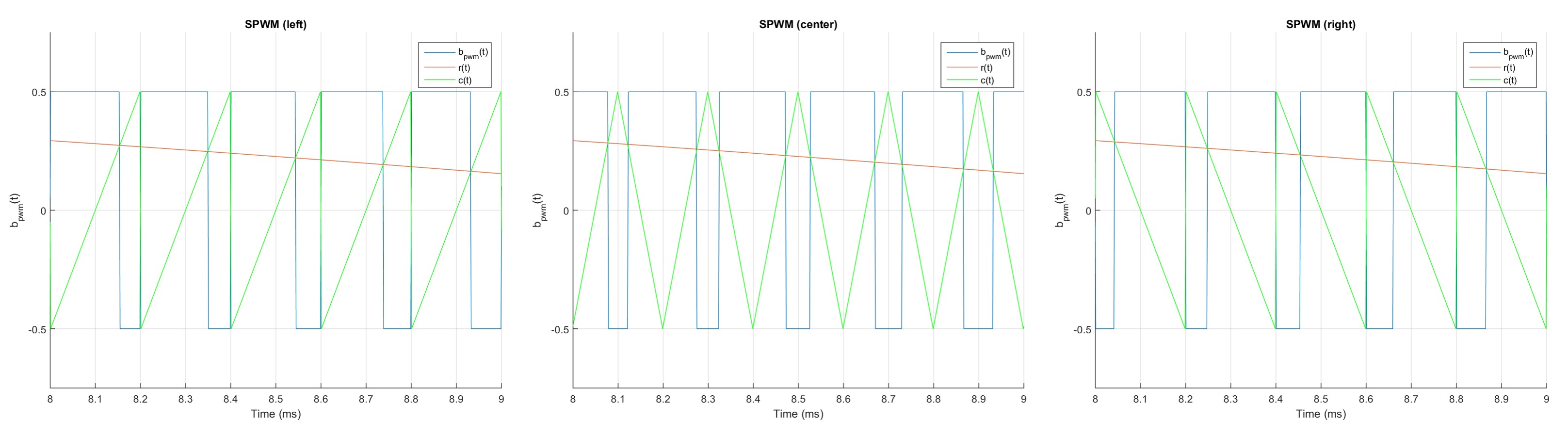
This relationship, copied-and-pasted over multiple $T$ intervals, yields the sawtooth-shaped carrier waveform $c(t)$, as drawn in the figure above, right. It now comes as fairly straightforward that $b_{pwm}(t) = a$ when $r(t) > c(t)$ and $b_{pwm}(t) = 0$ otherwise. With a bit of wit, we can now write $b_{pwm}(t)$ generically as
\begin{equation}\label{eq:pwm} b_{pwm}(t) = a (\text{sign} [ r(t) – c(t) ]) \end{equation}
Neat and compact. This form is also know as natural PMW (or naturally sampled PWM). And, in case you’re wondering: there’s this obscure thing called uniform PWM, but I won’t be touching that. Ever.
Chop that sinewave… Julienne or Chiffonade?
By plugging the generic sinusoidal wave below
\begin{equation}\label{eq:rsine} r(t) = R_0 + R_1 cos(2\pi f_1 + \theta_1) \end{equation}
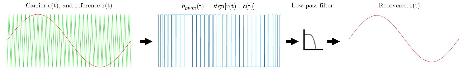
in our equation \ref{eq:pwm} above, we get this neat thing called Sinusoidal Pulse Width Modulation (SPWM). Following the intuition developed in the last section, SPWM generates a waveform with the harmonic content of the desired sine wave, as shown in the figure below. I mean, that PWM signal looks like a jumbled mess, but it has the harmonics we’re looking for, believe me. Low-pass-filtering the signal will reveal the modulated sine wave.
The very attentive may have noticed that, in the above picture, the carrier wave $c(t)$ (in green), is not a sawtooth wave as previously defined, but a triangular wave. In actuality, if we follow the intuition outlined in the previous section, we’ll notice that any triangle-shaped $c(t)$ produces the same $A_0 = A_s$ area equivalence. In practical applications, however, only three different carrier waveforms are used, which yield three basic PWM schemes:
- Sawtooth: trailing-edge modulation, or left-aligned PWM (figure below, left)
- Triangular: double-edge modulation, or center-aligned PWM (figure below, center)
- Inverse sawtooth: leading-edge modulation, or right-aligned PWM (figure below, right)
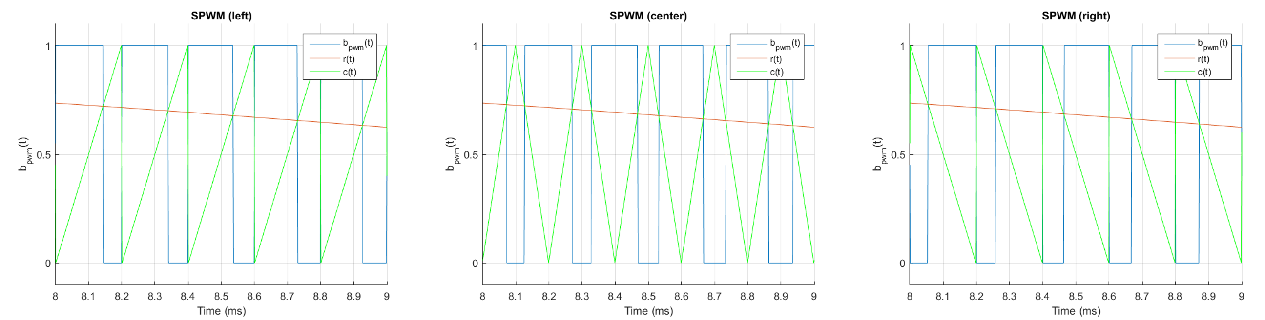
When I faced this carrier-wave-palette for the first time, my initial question was, “ok, cool. So which one do I pick? Is there any difference?”. As it turns out, there’s always some debate over which one to use, but fairly little quantitative approaches to the issue. From an implementation perspective, a triangular carrier wave is a bit more of a hassle. On an MCU, a sawtooth wave can be tipically spawned by a counter that simply counts up and overflows. A triangular wave, on the other hand, requires said timer to go up, then down again. This means that, for a set carrier wave frequency, you have to either provide such counter with a clock signal twice as fast, or sacrifice one bit in the counter’s resolution. But beyond that, is there any modulation strategy that reduces undesired harmonics in the output signal?
This question is relevant for a couple reasons. First, VFD output isn’t usually filtered before it gets to the load – in fact, the load itself acts as a filter. In the case of an induction motor as load, the coils act as RL-filters, smoothing out the input current. Still, lots of undesired harmonic content in the signal might reduce efficiency, produce heat, and cause vibration and audible noise due to magnetostriction.
… but if you judge a fish by its ability to modulate a wave …
Cool. So, at this point, the goal is very clear: evaluate the VFD output from different PWM schemes. But evaluate according to what? Let’s pick two neat ones: harmonic content and total harmonic distortion.
Harmonic Content
We are clearly interested in evaluating which harmonics appear on each PWM scheme. My first thought was to look at the $C_n$ coefficients of the compact trigonometric Fourier series, as defined in equation \ref{eq:trigfourier} below.
\begin{align} \label{eq:trigfourier} f(t) = C_0 + \sum_{n=1}^{\infty} C_n \text{cos}(n\omega_0t + \theta_n) \end{align}
Unfortunately, things are a bit more hairy than that. If we take a look at the PWM equation \ref{eq:pwm} above, we see the obvious fact the function is periodic in both $r(t)$ and $c(t)$. To apply the Fourier definition above, we’d need to come up with a closed form for a single period of $\text{sign} [ r(t) – c(t) ])$, which is clearly algebraical masochism (or suicide). In order to analytically analyze the Fourier expansion for such a function, we need to introduce the Double Fourier Series Method: for any function $f(x, y)$, periodic in both $x$ and $y$, with a period of $2\pi$ in both axes* we can write:
\begin{align}\label{eq:doublefourier} f(x, y) &= C_{00} + \sum_{n=1}^{+\infty}C_{0n} \text{cos}(ny+\theta_{0n})+ \sum_{m=1}^{+\infty}C_{m0}\text{cos}(mx + \theta_{m0}) \notag \\ &+ \sum_{m=1}^{+\infty}\sum_{n=\pm1}^{\pm\infty}C_{mn}\text{cos}(mx + ny + \theta_{mn}) \end{align}

Well, first off, for all the math inclined folks out there: sorry, but I’m not touching this with a ten foot pole – I’ll be going down the numerical route. However, if you do wish to check out its analytical expansion for various PWM strategies, check this document. Regardless, looking at this expression does provide us with some neat insight about what we should expect to see: the first term on the right-hand side of equation \ref{eq:doublefourier} represents a DC component, while the second and third terms represent the harmonics of both $y$ and $x$, respectively – these are identical to the one-dimensional Fourier Series in equation \ref{eq:trigfourier} above. More interesting, however, is the fourth term in that expression. It expresses the sideband frequencies that are generated as a result of the modulation process. We see that $n$ assumes positive and negative integer values, thus yielding upper- and lower-sideband (USB and LSB) spectra around each main harmonic of the carrier frequency.
*If we want \ref{eq:pwm} to fit this criterion, we could write it as $b_{pwm}(t) = f(x, y) = \text{sign}[r(x) – c(y)]$, $y = 2\pi f_1 + \theta_1$, $x = 2\pi f_c + \theta_c$, where $f_c$ is the carrier’s frequency and $f_1$ is the modulated sine’s frequency.
Total Harmonic Distortion
While the Fourier series gives us detailed information on the signal’s harmonics, the Total Harmonic Distortion (THD) factor gives us a handy ratio between the harmonics we care about, and the ones we do not. As mentioned, we are interested in producing a pure sine wave, and as such, we care about only a single fundamental harmonic – everything else may be properly labeled as distortion. Our THD can thus be expressed as
\begin{equation}\label{eq:thd} \text{THD}_F = \frac{\sqrt{\sum_{n=2}^\infty v_n^2}}{v_1} \end{equation}
where $v_n$ is the amplitude of the n-th harmonic and the F in “$\text{THD}_F$” stands for fundamental. Pure sine waves have a $\text{THD}_F = 0$, square waves have a $\text{THD}_F = 48.3\%$ (percent is a common representation for THD), and higher factors indicate higher distortion – in our case, meaning that less power is going were it should.
Three-sum
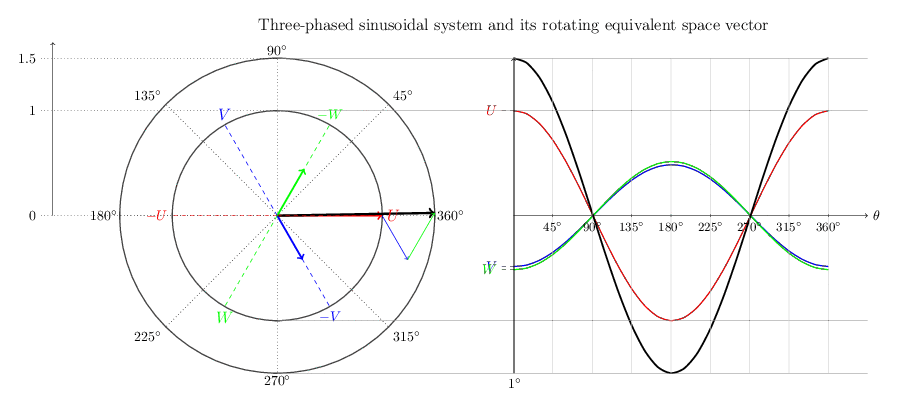
Naturally, we are interested in performing the aforementioned evaluations on the VFD’s output. To that end, our last missing ingredient is a means of properly combining the signals of the U, V and W legs into a single output signal. As discussed in the introduction, we are interested in three-phase AC inputs and outputs. Such signals can be easily visualized as a phasor projected onto three base vectors, 120º degrees apart** – each projection representing an individual phase. Well, since a picture is worth a thousand words, let the shamelessly stolen GIF below talk for itself:
In order to properly compute the magnitude of the rotating equivalent vector above (in black), we need to to represent it in an orthonormal basis (as we see above $\{U, V, W\}$ only span $\mathcal{R}^2$, and hence do not fulfill the criteria for orthonormality). Let’s thus pick the $\{\alpha, \beta\}$ vectors below as our new basis:
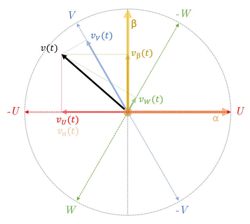
The choice of $\{\alpha, \beta\}$ is arbitrary (as long as they are orthonormal), but done to simplify upcoming calculations (since $\alpha$ represents the real part of the signal, and $\beta$, its imaginary part). Now, with a bit of trigonometry, we can represent a periodic signal $v(t)$ shown above in our new base:
\begin{equation} \label{eq:clarke} v(t) = \begin{bmatrix} v_{\alpha} \\ v_{\beta} \end{bmatrix} = { \frac{2}{3} } { \small \begin{bmatrix} 1 & -1/2 & -1/2 \\ 0 & \sqrt{3}/2 & \sqrt{3}/2 \end{bmatrix} } \begin{bmatrix} v_U \\ v_V \\ v_W \end{bmatrix} \end{equation}
This relationship is know as the Clarke transform, and is frequently used in the analysis of three-phase AC circuits. Let’s now assume that the U, V and W phases are each producing individual SPWM signals as per the equation $\ref{eq:pwm}$, all 120º degrees apart from each other (figure below, right) – notice that the phases’ outputs were normalized to the $[0, 1]$ range. We can now combine them via our definition \ref{eq:clarke} above, to produce the actual output signal of our VFD (real part $\alpha$ drawn in the figure below, right):
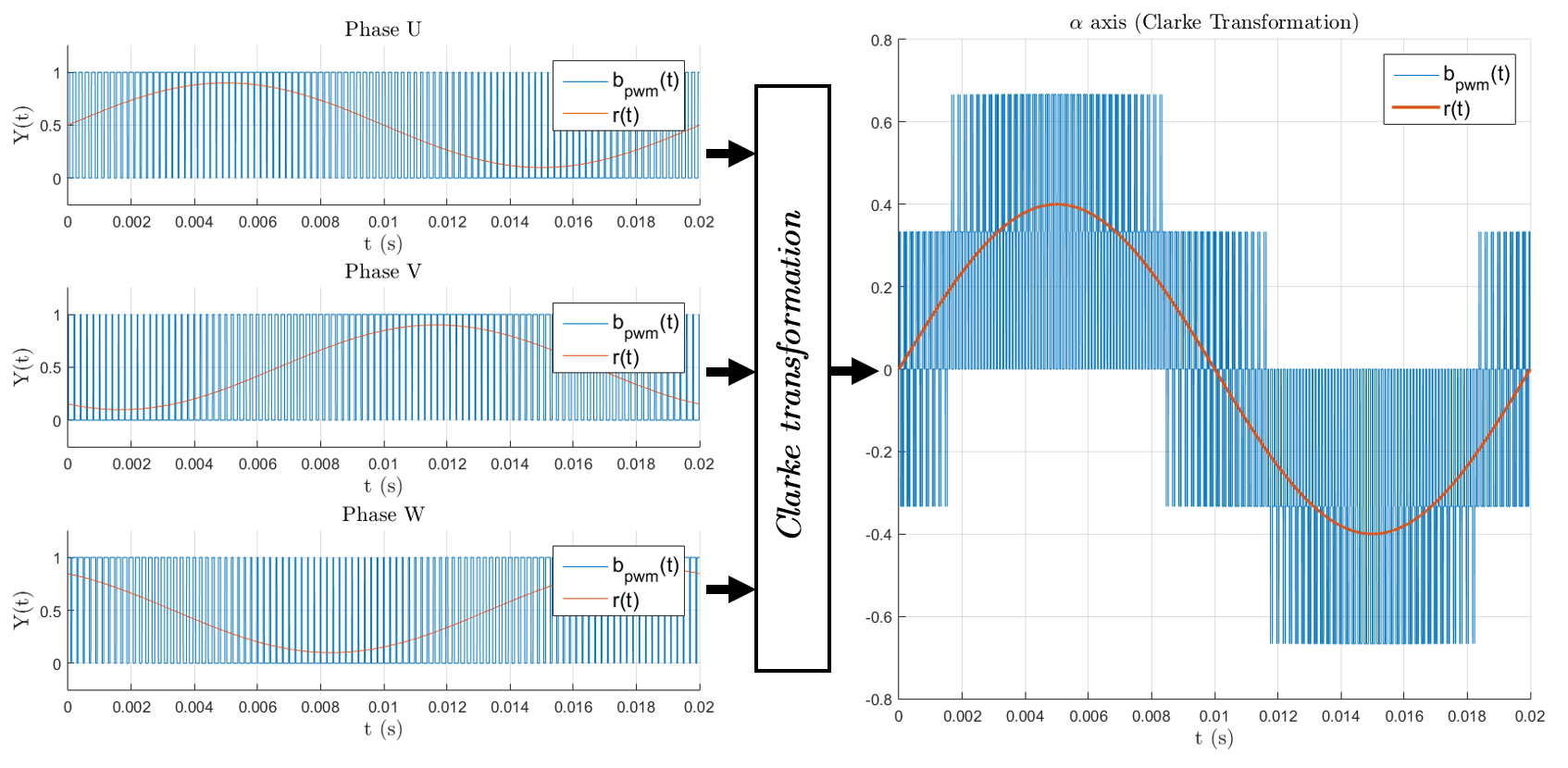
It is worth noting how each phase is capable of producing only unipolar signals – i.e., signals ranging from 0V to the $V_{DC}$ voltage of the VFD’s DC bus. Their combined output, however, yields true bipolar output. While this might be slightly counter-intuitive at first, imagine all three phases producing a steady PWM signal with a 50% duty cycle. This “balance point” produces zero output (since $V_\alpha = 1*0.5 – 1/2*0.5 – 1/2*0.5 = 0$, as per equation \ref{eq:clarke}). From this state, by changing the value of one or more phases, we can produce arbitrary output vectors with magnitudes ranging from $-2V_{DC}/3$ to $2V_{DC}/3$. For a bit more discussion on that topic, check this out.
**In case you’re wondering, this 120º offset between the phases is ultimately related to the physical placement of the stator windings inside three-phase motors and generators.
Last, but not least
We are finally ready to answer the question we posed several paragraphs ago: which PWM strategy is best? Left-aligned, right-aligned or center-aligned?
First off, as we’ve discussed before, our evaluation tools only care about the frequency spectra of our signals. So, taking into account the time reversibility of the Fourier series, and noting that left- and right-aligned SPWM waveforms are mirror images of each other, we immediately know that they’re equivalent (for our intents and purposes). So, we’ll only compare trailing-edge and double-edge modulations.
To generate the SPWM signals, I’ve implemented the SPWM definion (i.e., combining equations \ref{eq:pwm} and \ref{eq:rsine}) in Matlab (Code!). Computing the Fourier single-sided amplitude spectrum (Code!), as well as computing $\text{THD}_F$ (Code!) was also done in Matlab. [Any feedback on the correctness of these code snippets would be greatly appreciated] The generated plots are shown below. U, V, and W phases are modulating a 50Hz sinewave with an amplitude modulation index of 0.8, on a 5kHz carrier (identical as shown in the figure above, left), so the expected output amplitude waveform is $0.8*0.5 = 0.4$:
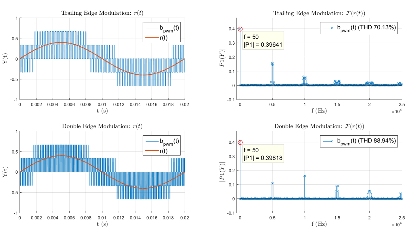
And, voilà. We immediately see that in both modulation schemes, the desired fundamental is there, almost perfectly in the desired amplitude ($0.39 \approx 0.4$) – yey! all that SPWM hassle does work after all. Now, interestingly, we have a rather curious result with the FFT spectra and the THD factors. At first, we see that Trailing-Edge modulation has a somewhat smaller distortion factor (70.13%), but its spectrum seems arguably more messy. Moreover, we can see that Double-Edge modulation seems to have much less harmonic content (in fact, it has exactly half of the sideband harmonics, as verifiable if we expand equation \ref{eq:doublefourier} analytically for each scenario, as seen here). On top of that, the fundamental switching harmonics (around 5kHz) have smaller amplitudes in the Double-Edge scheme. So, what gives?
It seems that the higher-order harmonics of the Double-Edge modulation tend to weight-in more heavily in the quadratic sum of the THD factor, yielding a higher overall distortion (88.94%). In practice, however, the RL-filter-characteristic of VFD loads will have a cutoff frequency around the hundreds of Hz, so realistically, harmonics above the switching frequency will have almost no effect***. So, we can confidently argue that, in practical applications, Double-Edge modulation – a.k.a. center-aligned PWM – does produce less harmonics, which seems to echo the faint opinions on the topic that float around the interwebs.
Now, of course: as the image above shows, the difference isn’t all that extreme, and as we’ve discussed above, there’s a bit more implementation effort associated with center-aligned PWM. So, once again – and slightly disappointingly – YMMV.

***Very broad and oversimplified generalization. Don’t sue me if you fry your setup testing something I’ve said.
Disclaimer (& closing thoughts)
Well, let’s just make it very clear: this whole thing is a somewhat brief write-up of my latest incursions in what’s an unknown territory for me. I’ve been figuring stuff out on the fly, so if you spot anything wrong, please, let me know!
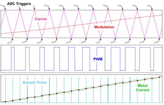
Edit: In a recent conversation, a friend of mine and a literal master of all-things-electric, Julio, added some very relevant information to this mix. He confirmed that, in practical applications, the choice of carrier waveform is not of great impact. However, when implementing a VFD (e.g. on a MCU) with any kind feedback control loop, the peaks and valleys in the triangular carrier of the center-aligned PWM can be used to synchronize ADC samplings of the generated waveform (figure below). This ensures that the sampling doesn’t happen during switching, reducing measurement noise (and, in case of current measurements, providing that pulse’s average value). This article goes into more depth into that, and it’s worth taking a look. He also mentioned that sawtooth carriers (in trailing- and leading-edge modulations) essentially synchronize the switching in all phases. This increases output noise due do parasitics in the circuit/load (stuff that we did not capture in this write-up), and can be a real issue in high-power applications. Thanks for the insight, Julio!
’til next time.